Nanoimprint
AutoSCIL
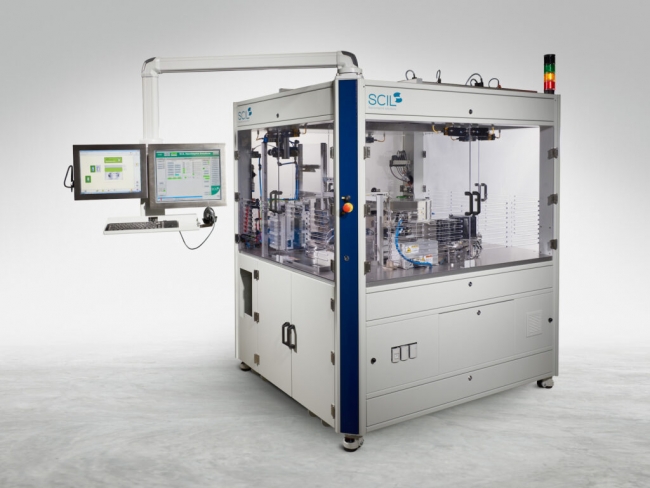
 SCIL Nanoimprint solutions offers NIL manufacturing solutions in a large variety. From manual R&D tools to fully automatic cassette-to-cassette systems and from 2” up to 300 mm wafers.
The manual R&D tools and automatic systems use the same imprint module which allows easy transition from manual to semi-automatic and fully-automatic processing.
Key features
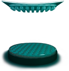
⦿Tri-layer stamp construction allows conformal contact printing even on non-flat and bowed surfaces.
⦿Unique SCIL imprint process ensures sub 10 nm resolution with low pattern deformation and no stamp damage by particles.
⦿Overlay alignment < 1 µm
⦿The excellent etch properties of the sol-gel resist result in high etch rates.
⦿The thermal stability﹐ optical transparency and (UV) stability of the sol-gel makes it suitable as functional layer.
⦿Use of thermal sol-gel increases stamp lifetime.
⦿Overall combining highest imprint quality and yield with high throughput and low total cost of ownership.
The fully automatic systems include all essential process steps in a closed coupled system: wafer handling﹐ pre-aligning﹐ spin-coating﹐ SCIL imprinting﹐ baking and cooling.
⦿Specifications
Imprint method SCIL low pressure softstamp NIL
Capacity
30 – 60 wafers/hour depending on wafers size﹐ wafer material﹐ pattern dimensions and material process
Wafer size 2” up to 200 mm
Wafer material Glass﹐ Silicon﹐ Sapphire﹐ GaAs﹐ other
Wafer thickness 0.3 – 1.7 mm
Wafer handling Cassette-to-cassette﹐ pre-aligning﹐ robot handling
Resist types Thermal sol-gel (NanoGlass T-series)
UV sol-gel (NanoGlass UV-series)
UV organic (NanoSynth UV-series)
Resist coating Integrated spin coating system
Post processing Baking and cooling
Overlay alignment X﹐Y alignment accuracy < 1 µm