Home > SEMICONDUCTOR > Reliable 3D and 2D Measurements for Multi-process > Measuring System WAFERinspect
Reliable 3D and 2D Measurements for Multi-process
Measuring System WAFERinspect

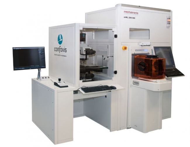
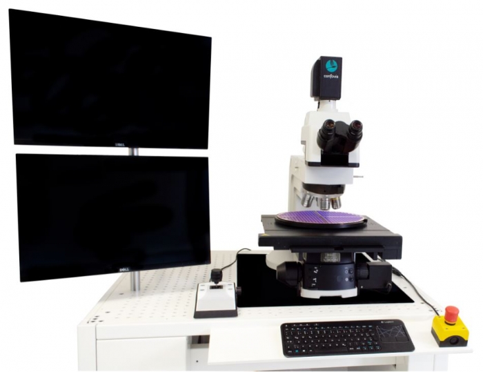 The Confovis WAFERinspect system is suitable for a detailed 3D and 2D measurement of microstructures. It combines confocal 3D measurements﹐ classical 2D measurements and visual inspection﹐ which allows an analysis of different process steps within the semiconductor production.
•High-precision measuring technique: confocal with high vertical resolution of < 3 nm (VDI 2655)
•Measuring and working range up to 300 mm: suitable for all wafer sizes from 2“– 12“ (semi standard)
•2D inspection: measurement of critical dimensions (Line/Space﹐ VIAs) and Overlay﹐ defect review (also with KLA-File)﹐ Cognex or Halcon interface for “non-standard” challenging 2D measurements
•3D inspection: for any kinds of structures (roughness﹐ step height﹐ slopes﹐ bumps﹐ saw cuts﹐ TSVs) and surfaces (silicon﹐ resist﹐ epoxy﹐ glass﹐ chrome)
•Fully automatic measurements also on difficult wafer types (MEMS﹐ Thin﹐ Taiko﹐ Warped﹐ Frame)
•Wafer handling systems and wafer positioning systems available (flexible wafer sizes and types﹐ frame handling etc. possible)
•Measuring by recipe: automated measurements for all measuring tasks
•Functionality of a traditional microscope