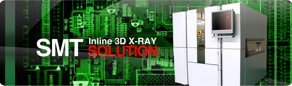
LASER Debonding Equipment
LASER Debonding Equipment
雷射解離設備

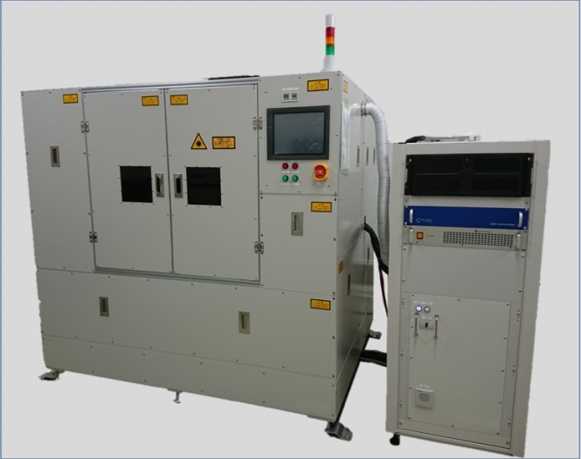
This LASER debonding equipment is used for a semiconductor packaging process or manufacturing process for ultra-thin semiconductors to peel off a temporary bonding layer with a LASER beam without stress.
Using a pulse LASER with a LASER beam wavelength of 355 nm licensed from IBM﹐ this equipment ensures that the LASER beam is absorbed only on the surface of a temporary resin layer﹐ thus curtailing damage to the device.
It supports FOPLP of large panel size﹐ achieving uniform LASER irradiation for workpieces of up to 600 mm2.
此雷射解離設備用於半導體封裝製程或超薄半導體的生產製程,以利用雷射解離臨時接合層。
此設備使用IBM許可波長為355 nm的雷射光束的脈衝雷射,可確保雷射光束僅在臨時樹脂層的表面上被吸收,從而減少了對設備的損壞。
它支持大面板尺寸的FOPLP,可對最大600 mm2的工件實現均勻的雷射照射。
用途:
・ A temporary bonding process for forming semiconductor packaging
・ A temporary bonding process for forming a semiconductor re-distribution layer (RDL)
・ A temporary bonding process for forming an ultra-thin semiconductor
・ Other processes using temporary bonding
・半導體封裝成型臨時接合製程
・半導體再分配層(RDL層)的成型臨時接合製程
・超薄半導體成型臨時接合製程
・其他涉及臨時接合的製程