Home > SEMICONDUCTOR > X-ray Bump / Void Inspection Equipment > X-ray bump/void Inspection Equipment Six-2000/3000
X射線凸點/氣泡檢查設備
X-ray Bump / Void Inspection Equipment
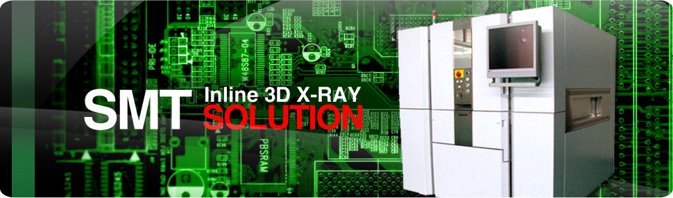
X-ray bump/void Inspection Equipment Six-2000/3000
X射線凸點/氣泡檢查設備

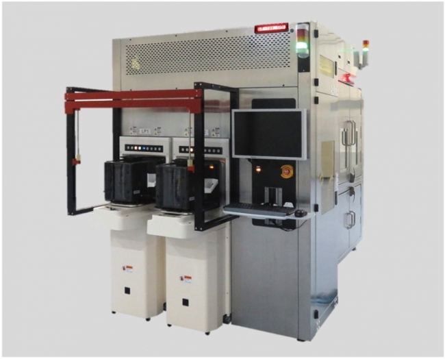
Equipment to inspect/judge bumps on the wafer automatically.
By transmitting X-rays through voids (air bubbles) inside the wafer﹐ the void diameter (area) is calculated from a transmitted image to automatically judge whether to accept voids exceeding standards.
It uses a microfocus X-ray tube as an X-ray source﹐ and a cutting-edge X-ray digital camera for the X-ray image receiving section﹐ to extract high-resolution images and enable high-precision void inspection.
自動檢查/判斷晶圓凸點的設備。
通過使X射線穿過晶片內部的空隙(氣泡),可以根據所透射的圖像計算空隙直徑(面積),從而自動判斷是否接受超過標準的空隙(氣泡)。
它使用微焦點X射線管作為X射線源,並使用尖端的X射線數位照相機作為X射線圖像接收部分,以提取高分辨率圖像並實現高精度的空隙(氣泡)檢查。
用途:
・ Inspection of bumps on silicon wafers
・ Inspection of soldered areas such as BGA on mounted substrates
・ Inspection of soldered areas flip-chip-mounted on LED
・ Inspection of voids on two-layer soldered areas of power devices (IGBT)
・檢查矽晶片上的凸起
・檢查封裝基板上的BGA等焊接區域
・檢查LED的FlipChip封裝上的焊接區域
・檢查功率器件(IGBT)兩層焊接區域的空隙(氣泡)