Vision Systems
Microscope Scanner

Microscope Scanner (LEDs﹐ OLEDs﹐ MEMS)
Raise the efficiency of your production
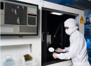
The microscope scanner for the inspection of LEDs﹐ OLEDs and MEMS is based on an automated platform﹐ which delivers a high throughput of the parts. The basic system consists of a handling unit and a measuring unit. In the handling unit﹐ a robot transports the wafers or substrates﹐ which can exhibit diameters of up to 12"﹐ out of the cassettes﹐ while in the measuring unit the samples are moved under the detector. Typically﹐ resolutions of 0.1 μm - 5 μm are achieved in combination with illumination techniques from the UV-VIS-IR spectral range.
Performance data and key facts
The inspection of components is necessary in the production of
LEDs
OLEDs
MEMS
Diodes
Customized products
Typical inspection objectives are
Surface and volume defects (microcracks﹐ scratches﹐ bumps﹐ flaking﹐ particles﹐ inclusions)
Evaluation of structures (component arrangement﹐ laser pattern﹐ etching processes﹐ interconnects)
The measuring unit can be equipped with special detectors﹐ lightings and types of excitations such as
Fast line scan and matrix cameras with high resolution (up to 0.5 μm / px)
Different contrast modes (BF﹐ DF﹐ DIC﹐ Pol)
Optical illumination from UV to IR
Luminance and color measurement
Interferometry
Photoluminescence
Electroluminescence
Thermography
Raise the efficiency of your production
The microscope scanner for the inspection of LEDs﹐ OLEDs and MEMS is based on an automated platform﹐ which delivers a high throughput of the parts. The basic system consists of a handling unit and a measuring unit. In the handling unit﹐ a robot transports the wafers or substrates﹐ which can exhibit diameters of up to 12"﹐ out of the cassettes﹐ while in the measuring unit the samples are moved under the detector. Typically﹐ resolutions of 0.1 μm - 5 μm are achieved in combination with illumination techniques from the UV-VIS-IR spectral range.
Performance data and key facts
The inspection of components is necessary in the production of
LEDs
OLEDs
MEMS
Diodes
Customized products
Typical inspection objectives are
Surface and volume defects (microcracks﹐ scratches﹐ bumps﹐ flaking﹐ particles﹐ inclusions)
Evaluation of structures (component arrangement﹐ laser pattern﹐ etching processes﹐ interconnects)
The measuring unit can be equipped with special detectors﹐ lightings and types of excitations such as
Fast line scan and matrix cameras with high resolution (up to 0.5 μm / px)
Different contrast modes (BF﹐ DF﹐ DIC﹐ Pol)
Optical illumination from UV to IR
Luminance and color measurement
Interferometry
Photoluminescence
Electroluminescence
Thermography