Vision Systems
Bare Wafer Inspection

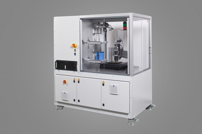
 Wafer Inspection System AQUILA
■ Raise the efficiency of your production ■
For more than two decades Intego has been offering standard and customized optical inspection systems for wafer production. The production of flawless wafers with continuous yield improvement is a top priority of the semiconductor industry. Early detection of damaged wafers not only saves unnecessary process time﹐ but also long and expansive downtimes due to wafer breakage.
Depending on the production step different inspection systems are available. Besides the classical surface inspection systems for the front and back side of the wafer﹐ Intego also offers special solutions for the detection of microcracks and a novel 100 inspection of the wafer edge and notch region. The systems are characterized not only by their innovative inspection solutions﹐ but also by their custom-made handling concept and the comprehensive defect analysis and review software.
■ Surface inspection
- full-wafer front and back side inspection
- fast micro and macro defect inspection
- etch pit density analysis of defect-selective etching
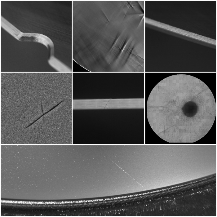
- detection of handling scratches﹐ saw marks﹐ grinding traces﹐ pin holes﹐ particles﹐ stains﹐ etc.
■ Edge inspection (LYNX)
- highly sensitive 100 edge and notch inspection
- multi-angle inspection configuration perfectly adapted to edge profile
- measuring wafer profile and thickness
- detection of chipouts﹐ cracks﹐ scratches﹐ saw marks﹐ grinding marks﹐ residues﹐ etc.
■ Material inspection
- sophisticated illumination concepts (e.g.﹐ UV-PL﹐ NIR)
- clear differentiation between surface and internal defects
- wafer robot or conveyor belt handling solution
- detection of microcracks﹐ polytypes﹐ inclusions﹐ crystal defects﹐ etc.
■ Some general performance data
▼ Application
- as-cut﹐ grinded and mirror-polished wafers
- inspection of opaque﹐ semi-transparent and transparent wafers up to 300 mm
- solutions for Si﹐ SiC﹐ GaN﹐ GaAs﹐ Ge﹐ sapphire﹐ glass﹐ etc. available
▼ Technology
- image acquisition perfectly adapted to the wafer material﹐ size﹐ shape and motion
- different focus﹐ magnification and illumination in just one cycle
- inspection options with bright- and darkfield﹐ transmitted light﹐ laser scattering﹐ polarization﹐ photoluminescence﹐ DIC﹐ etc.
- illumination configuration options from UV to IR
- high resolution tool configurations up to 0.1 µm/px available
▼ Handling
- inspection systems either manually loaded or automated with OHT or AGV
- customized EFEM by Intego or other standard suppliers up to four load ports
- open cassette﹐ FOSB﹐ FOUP and/or SMIF based handling﹐ also mixed loading possible
- vacuum or edge-grip handling﹐ flipper﹐ aligner and ID scanner available
- automatic wafer sorting based on inspection results
▼ Software
- proprietary automatic defect detection and classification algorithms (online/offline)
- advanced manual revaluation of previous defect mappings
- advanced wafer defect analysis﹐ review and binning ability
- customizable GUI﹐ result visualization﹐ KLARF reporting and SQL data bank solutions
- SEMI software interface including SECS/GEM