Vision Systems
Epitaxial and Patterned Wafer Inspection

 ■ Raise the efficiency of your production ■
In the production of epitaxial layers﹐ a variety of different defects can occur due to imperfect substrate quality﹐ process-related contamination and the coating process. For their safe and reliable detection﹐ various sophisticated inspection methods are available. In particular﹐ photoluminescence and DIC microscopy enable the reliable detection of the critical crystallographic defects﹐ which in certain cases can lead to component failure if not detected in time.
Detection of exposure and implantation errors as well as the control of overlay offset and CD values are of crucial importance for the complex manufacturing of microelectronic products. Intego’s inspection and measurement systems are also supported by its proprietary CAD based defect detection and wafer yield prediction software. In addition to the classical evaluation algorithms﹐ advanced neural networks for defect detection and classification are also available.
■ Unpatterned epiwafer inspection
- simultaneous front and back side inspection
- fast micro and macro defect inspection
- inspection with maging techniques like laser scattering﹐ PL and DIC for sub-micron sensitivity
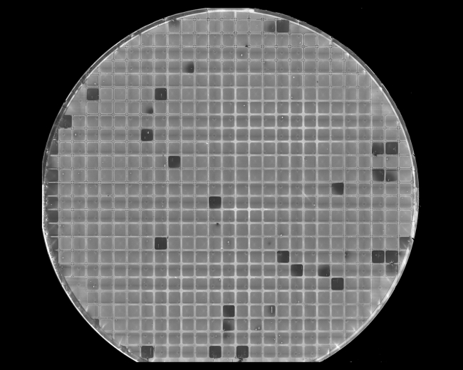
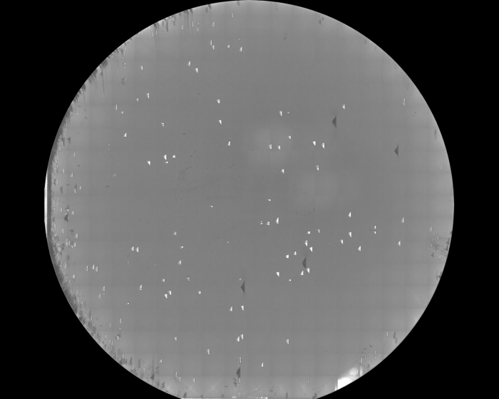
- detection of pits﹐ bumps﹐ particles﹐ coating defects﹐ color variation﹐ etching residues﹐ haze﹐ stacking faults﹐ triangles﹐ carrots﹐ basal plane dislocations﹐ slip lines﹐ etc.
■ Patterned wafer inspection
- inspection of partially processed wafers including laser micro-processing
- CAD based 2D defect detection and metrology solutions
- detection of surface and crystallographic defects as well as exposure and implantation errors﹐ overlay errors and die shifts including critical dimension (CD) measurements
- wafer yield prediction based on advanced defect classification algorithms
■ Some general performance data
▼ Application
- inspection of opaque﹐ semi-transparent and transparent wafers up to 300 mm
- solutions for Si﹐ SiC﹐ GaN﹐ GaAs﹐ Ge﹐ sapphire﹐ glass﹐ etc. available
▼ Technology
- image acquisition perfectly adapted to the wafer material﹐ size﹐ shape and motion
- different focus﹐ magnification and illumination in just one cycle
- Inspection options with bright- and darkfield﹐ transmitted light﹐ laser scattering﹐ polarization﹐ photoluminescence﹐ spectrometry﹐ DIC etc.
- illumination configuration options from UV to IR
- high resolution tool configurations up to 0.1 µm/px available
■ Handling
- standard EFEMs with customized functionality available
- open cassette﹐ FOSB﹐ FOUP and/or SMIF based handling﹐ also mixed loading possible
- custom-tailored vacuum and edge-grip chuck designs and mini-environment solutions
- vacuum or edge-grip handling﹐ flipper﹐ aligner and ID scanner available
■ Software
- proprietary and deep learning defect detection and classification algorithms
- advanced manual revaluation of previous defect mappings
- advanced wafer defect analysis﹐ review and binning ability
- customizable GUI﹐ result visualization﹐ KLARF reporting and SQL data bank solutions
- SEMI software interface including SECS/GEM