Vision Systems
Applications in Semiconductor

 Applications in Semiconductor: SOLAR﹐ CERAMICS & GLASSES﹐ PLASTICS﹐ METALS﹐ ELECTRONICS
■ Raise the efficiency of your production ■
The demand for customized optical inspection systems is constantly increasing. A new production process﹐ a new product or the occurrence of a new type of defect often requires an adapted solution. For more than 20 years Intego has been developing customized wafer inspection and metrology systems for the front-end and back-end area in close cooperation with its customers. Requirements for throughput﹐ handling﹐ interfaces﹐ SEMI conformity﹐ and cost of ownership are considered in the same way during the development phase as the optical inspection technology﹐ which is the heart of the system. In the end﹐ the customer receives a customized inspection system that meets his requirements in the best possible way and thus makes a permanent contribution to improved product quality and productivity.
Special inspection topics are:
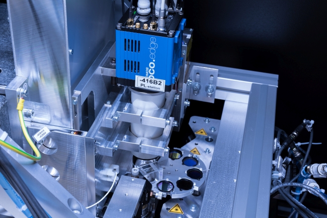
■ UV to NIR photoluminescence (AQUILA PL): defect detection and material characterization in the field of opto- and power electronics (e.g. LED﹐ SiC﹐ GaN)
■ Spectrometry: advanced crystal defect classification for power electronic materials
■ Lifetime measurement (MODULUM): spatially resolved charge carrier lifetime measurements based on modulated luminescence
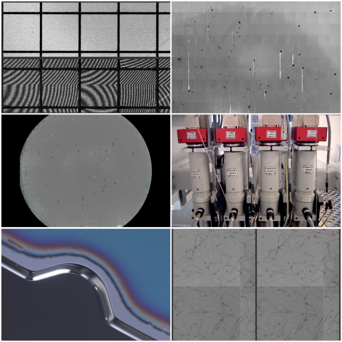
■ Infrared inspection: fast and high-resolution microcrack detection in semiconductor and MEMS wafers
■ Edge and notch inspection (LYNX): 100 wafer edge and notch inspection system using an unprecedented inspection concept
■ Surface inspection: fast and sensitive surface inspection using laser scattering﹔ reliable detection of particles down to 100 nm and smaller
■ Large and irregular shaped substrate and panel inspection: multi camera setups and customized handling solutions for the inspection of non-standard or oversized semiconductor substrates
■ Microcrack detection: highly sensitive optical crack detection in diced wafers (e.g. LED﹐ diodes﹐ MEMS)
We are very pleased to announce that our activity for a photoluminescence based wafer inspection system was awarded the Semikron Innovation Award 2016 at the power electronics conference PCIM in Nuremberg. The official press release can be found here .
■ Some general performance data
▼Application
- customized and flexible software and hardware solutions for wafer and die inspection
- optical inspection of opaque﹐ semi-transparent and transparent wafers
- configuration options for wafer size and shape up to 500 mm (round or square)
▼ Technology
- combining different inspection methods in just one system
- different focus﹐ magnification and illumination in just one cycle
- image acquisition optimized for multi-level inspection
- inspection options with bright- and darkfield﹐ transmitted light﹐ photoluminescence﹐ spectrometry﹐ laser scattering﹐ polarization﹐ interferometry﹐ thermography﹐ DIC etc.
- illumination configuration options from UV to IR
- high resolution tool configurations up to 0.1 µm/px available
▼ Handling
- customized EFEM by Intego or other standard suppliers with small footprint
- custom-tailored vacuum or edge-grip handling and chuck design
- special cleanroom and mini-environment solutions
▼ Software
- advanced image processing and algorithms based on state-of-the-art PC cluster solutions
- automatic inspection based on user-friendly CAD or golden sample comparison
- proprietary automatic defect detection and classification algorithms (online/offline)
- special pattern recognition and deep learning solutions available
- advanced wafer defect analysis﹐ review and binning ability
customizable GUI﹐ result visualization﹐ KLARF reporting and SQL data bank - solutions
- SEMI software interface including SECS/GEM