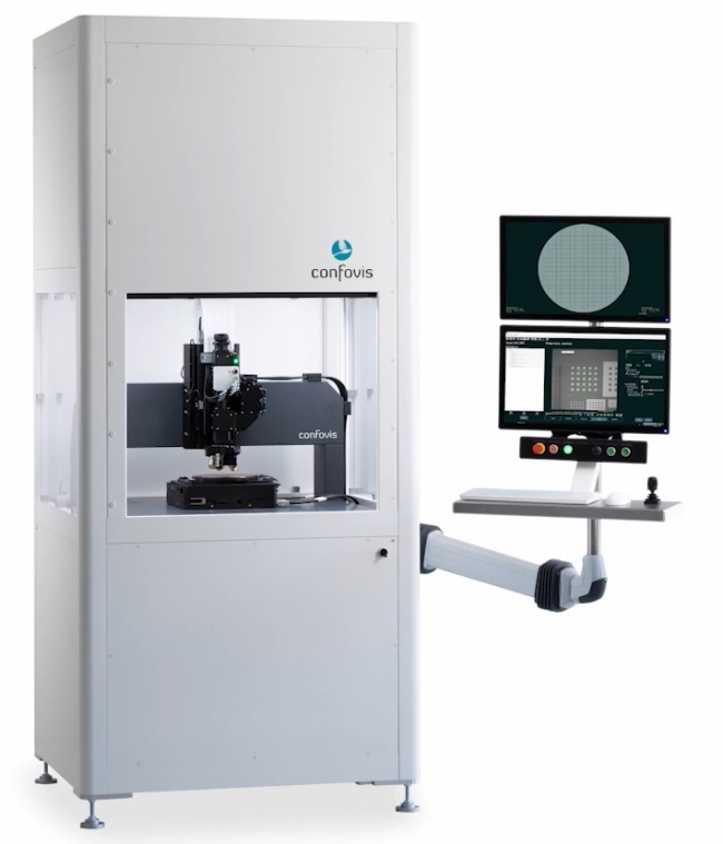
Reliable 3D and 2D Measurements for Multi-process
Wafer Inspection Systems

■ Defect detection and dimensional measurement increase output
Depending on the requirements of the structures to be produced﹐ wafers go through many individual process steps and sometimes remain within the wafer fab for weeks until production is completed. A wafer inspection by means of defect inspection and dimensional measurements excludes that incorrectly processed wafers continue to run through production. Wafer inspection with Confovis measuring systems helps to identify deviations in processes﹐ to find the cause and to correct it.
With the WAFERinspect measuring systems and the patented confocal optical measuring method (Structured Illumination Microscopy﹐ SIM)﹐ both defect detection and dimensional measurements are possible on one tool.
■ Confocal 3D measurements
- Independent of material: silicon﹐ epoxy﹐ glass﹐ chrome﹐ photoresist ...
- Artifact-free﹐ even demanding surfaces (no "bat wings")
- High speed : 60 confocal frames per second (250 million measuring points / s)
- Layer thickness / Film Thickness / Layer Stack
- topography
- Coplanarity
- Bumps
- Roughness
- Step Height
■ 2D measurements: Critical Dimensions
- Line / Space
- VIAs
- Oblong holes
- Overlay
■ Defect inspection
- Macro defects
- Micro defects
- Particle inspection
- Golden sample
- Artificial intelligence
- Neural Networks
■ Visual inspection
- Operator mode (visual inspection)
- Color images
- Depth of focus shots
- Stitching
- Documentation through comment function
- Digital inking
- Visual inspection with fine alignment﹐ KLARFF files