
Home > SEMICONDUCTOR > Reliable 3D and 2D Measurements for Multi-process > Automated Optical MEMS Inspection
Reliable 3D and 2D Measurements for Multi-process
Automated Optical MEMS Inspection

 MEMS achieve higher reliability than discrete sensors and actuators. This is due﹐ on the one hand﹐ to the omission of connectors and cables and﹐ on the other hand﹐ to the use of simple physical effects that enable short reaction times and functional paths.
During the inspection or MEMS measurement ﹐ these must be examined for defects ( defect inspection ) and the structures measured in 2D and 3D in order to control and control production processes. When measuring MEMS 3D in particular﹐ the Structured Illumination Microscopy (confocal microscopy) patented by Confovis comes close to the resolution and accuracy of atomic force microscopes (AFM)﹐ but is able to measure 100 to 1000 times faster. Another advantage of the Confovis measuring system is the material- independent 3D measurement﹐have difficulties with chromatic confocal sensors and white light interferometers. So too may combinations of materials such as gold and epoxy﹐ chrome on glass and polyimides on quartz are measured.
■ Confocal measurement: the advantages of the Confovis measurement method
Especially on wafers with very different structures and the required resolutions of less than 1 µm﹐ a MEMS inspection is challenging and usually cost-intensive. The optical measuring systems of confovis thanks to the use of microscope optics capable of the entire wafer surface on a large screen with shading correction﹐ but also "the-by the" analyze defects . By searching the 3D image stack for defects in the z-direction﹐ cracks in deeper layers can also be detected in multilayer MEMS structures ﹐ for example .
■ MEMS measurement: Reliably measure smaller MEMS structures
- Measurement of various surfaces and MEMS structures (e.g. plastic and gold)
- Unfiltered data / no measurement artifacts
- High and low reflectivity in one image field
■ A process control instrument for the inspection of MEMS structures
By integrating the defect detection into the high-resolution measuring system WAFERinspect ﹐ a process control instrument is created with which the defects can not only be recognized﹐ but also measured in 2D and 3D . This enables immediate conclusions to be drawn about their origin.
The data transfer to the host takes place via SECS / GEM.
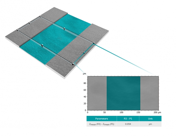
With MEMS inspection﹐ measurements are carried out with accuracies of 3 nm and repeat accuracies of 4 nm @ 3 sigma (example at a 50 nm level certified by the Physikalisch Technische Bundesanstalt). Also is precise measurement of angles﹐ distances﹐ radii ﹐ etc. possible. With Confovis﹐ customers have a universal and cost-efficient metrology platform at their disposal.