Home > SEMICONDUCTOR > Reliable 3D and 2D Measurements for Multi-process > Application in Semiconductor:
Roughness Measurement & Defect Inspection
Reliable 3D and 2D Measurements for Multi-process
Application in Semiconductor:
Roughness Measurement & Defect Inspection

■ Roughness Measurement: Measure the roughness of surfaces optically
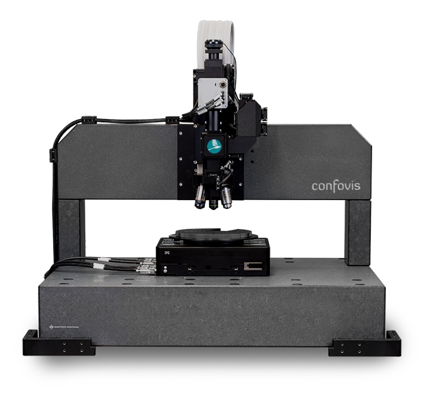
With the WAFERinspect measuring system from Confovis﹐ the customer has a universal and cost-efficient metrology platform at their disposal﹐ which integrates defect detection and 2D / 3D measurements in one system . The data transfer to the host takes place via SECS / GEM . The measurements are carried out with accuracies of 3 nm and repeat accuracies of 4 nm @ 3 sigma (example at a 50 nm level certified by the Physikalisch Technische Bundesanstalt). Precise measurement of angles﹐ distances﹐ radii﹐ etc. is also possible.
■ Defect Inspection:: In combination with 3D measurements
In order to better control and control production processes﹐ ( MEMS ) wafers﹐ microfluidic wafers﹐ etc. have to be examined for defects (defect inspection) and 2D and 3D measured ( wafer inspection ). By integrating the defect detection into the high-resolution measuring system WAFERinspect from Confovis﹐ a process control instrument is created with which the defects can be detected and all 2D and 3D structures can be measured .