Home > SEMICONDUCTOR > Micron Flip-Chip DIE BONDERS > MRSI-S-HVM 0.5-MICRON FLIP-CHIP DIE BONDERS - 0.5微米的覆晶黏晶機
Micron Flip-Chip DIE BONDERS
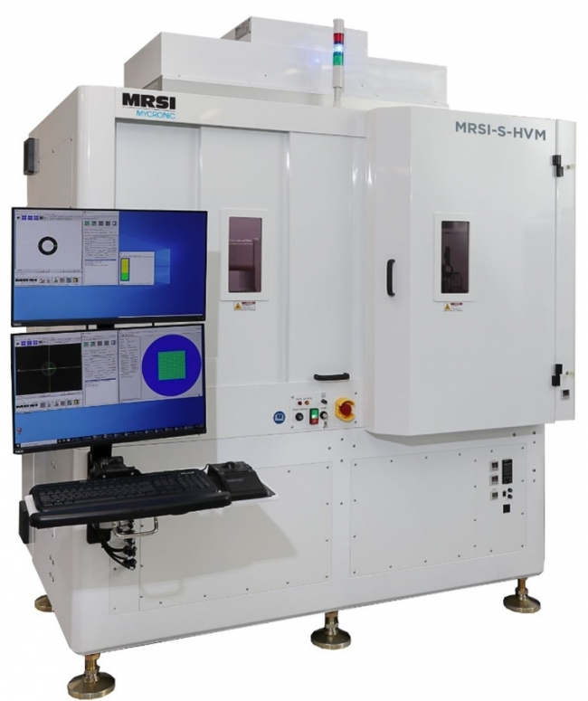
MRSI-S-HVM 0.5-MICRON FLIP-CHIP DIE BONDERS - 0.5微米的覆晶黏晶機

Applications & Features
• MRSI-S-HVM designed for integrated photonics volume manufacturing applications﹐ semiconductor wafer level packaging﹐ multi-chips﹐ multi-processes production in one machine.
• Designed for integrated photonics volume manufacturing applications﹐ semiconductor wafer level packaging﹐ multi-chips﹐ multi-processes production in one machine
• Two Modes with auto-change over: ±0.5μm @ 3σ and ±1.5μm @ 3σ﹔ both with on-axis z-force for die bonding. MRSI proprietary high z-force option available.
• Capable of Chip-on-Wafer (CoW)﹔ Chip-on-Interposer (CoI)﹔ Silicon photonics﹔ die from III-V wafer (8 inches) pick & place onto a silicon wafer (12 inches) and mapping
• Multiple processes﹐ including DAF﹐ eutectic﹐ epoxy stamping and dispensing﹐ thermal heating from top and bottom﹐ and MRSI proprietary bottom laser soldering.
• Flip chip bonding with direct alignment of fiducials on both bonding interfaces without additional reference or calibration required.
• MRSI proprietary wafer table with automated leveling.
• MRSI-S-HVM inherited all of the MRSI-HVM’s parallel processes using MRSI proprietary auto tool change and dual gantry/head.
• Material input methods include wafer﹐ Waffle pack﹐ and Gel-Pak®﹐ as well as customized fixtures.
Value to our Customers
• Industry-leading throughput﹐ superior flexibility﹐ and ultra-high-accuracy in high-volume﹐ high-mix manufacturing﹐ multiple process options
• With the switch between 0.5 micron and 1.5 micron modes there is an ability to balance the different accuracy chips/dies assembling within one machine to provide the best throughput and ROI for customers.
• Easy to use icon-based interface running on a Windows™ platform for ease of programming﹐ and low-cost machine maintenance.
• Industry-leading local technical support teams and application expertise
• 35+ years of experience in the industry with reliable 24/7 field operation
應用與功能
MRSI-S-HVM是為集成光子器件量產製造的應用而設計的,可用於半導體晶圓級封裝,多晶片、多工藝在一台機器上生產。
兩種模式自動切換: ±0.5 微米 @ 3σ,﹔ ±1.5 微米 @ 3σ,;兩者均具有Z軸向力控制的貼片模式﹐ 並可選MRSI專利的高壓力功能。
適用於晶片到晶圓封裝(CoW),晶片到仲介層的封裝 (CoI),以及矽光封裝。可從III-V族晶圓片(8英寸)提取晶片放置於12英寸晶圓片上,並可以記錄位置
支持多工藝:包括DAF、共晶、環氧蘸膠和點膠,可以使用頂部或底部加熱模式,及MRSI專利的底部鐳射加熱。
可直接對準倒裝晶片上和基板上的基準,不需要額外的參考點或校準。配有MRSI 專利的自動調平晶圓平臺。
MRSI-S-HVM繼承了MRSI-HVM所有便於並行工序的設計,包括MRSI專利的自動吸頭切換和雙龍門/貼片頭結構。
材料輸入方法包括wafer﹐ Waffle pack﹐ Gel-Pak®,以及定制的夾具。
對客戶的價值
行業領先的出貨量,卓越的靈活性,更多的工藝選項,和大批量高混合製造中超高的精度
通過在5微米和1.5微米模式之間自動切換,可以在一台機器內平衡不同精度的晶片封裝,為客戶提供最佳的生產能力和投資回報率。
Windows™平臺上運行的基於圖示的軟體介面,易於使用,便於程式設計和低成本維護。
行業領先的本地技術支援團隊和應用專家
超過35年的行業經驗保證了設備全天候可靠運行